Roll over image to zoom in
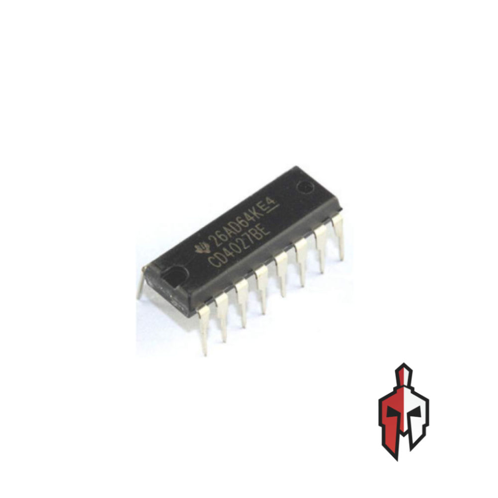
CD4027B JK Flip-Flop
Rs 90.00
Quick Info :
- Supply Voltage : 3V to 15V
- Input Voltage : 0V to V<sub>DD</sub>
- Output Voltage : 0V to V<sub>DD</sub>
- Clock Frequency : 5 MHz (at 10V)
- Propagation Delay : 60 ns (at 10V)
- Quiescent Current : 1 µA (max)
CD4027B is a single monolithic chip integrated circuit containing two identical complementary-symmetry J-K flip flops. Each flip-flop has provisions for individual J, K, Set, Reset, and Clock input signals. Buffered Q and Q signals are provided as outputs. This input output arrangement provides for compatibile operation with the RCA-CD4013B dual D-type flip-flop.
Specification :
- Type: Dual J-K Flip-Flop with Set and Reset
- Operating Voltage Range (Vcc): 3V-15V
- Output Voltage Levels:
- High Level Output (Voh): Vcc – 0.5V (minimum)
- Low Level Output (Vol): 0.5V (maximum)
- Input Voltage (Vin): 0V-Vcc
- Propagation Delay (tPLH / tPHL):
- Typically: 30 ns
- Maximum: 60 ns (depending on load)
- Power Dissipation (Pd): Max: 500 mW
- Supply Current (Icc):
- Typically: 1 mA
- Maximum: 10 mA (depending on load)
- Flip-Flop Reset and Set: Active LOW inputs for both Reset (R) and Set (S) pins
- Temperature Range: -40°C to +85°C
Reviews
There are no reviews yet.